More and more of human activity involves digital data. Managing the corresponding worldwide demand for increased data consumption and faster data processing can be helped by both fundamental and applied research on photonic systems. Photonic systems are unique because information can travel at the speed of light and can be relatively immune to environmental noise. Furthermore, individual light particles, i.e., photons, can act as an intermediary between quantum particles, and so photonic systems may be an important component in the realization of quantum computers which could dramatically speed up certain computational tasks, for example factoring the product of two large prime numbers as outlined by Shor's algorithm. One direction of research in this area called nanophotonics is to take advantage of nanofabrication techniques developed by the electronics industry to create novel nano-scale photonic structures for guiding and manipulating light.

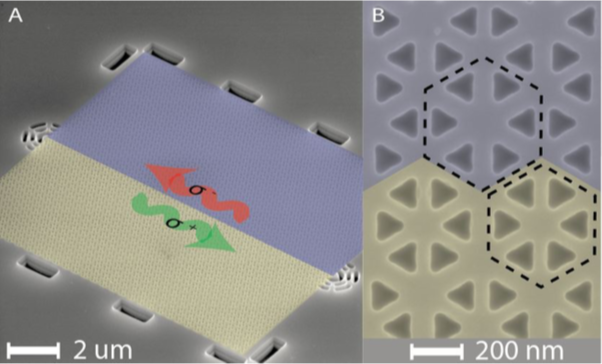
I worked in the area of nanophotonics at the University of Maryland and the Joint Quantum Institute to create novel photonic waveguide systems that can travel around corners without significant loss and are robust to fabrication imperfections. This will be important in the mass production of photonic integrated circuits with complicated circuit topologies. We realized this new photonic waveguide by engineering the topological properties of the photonic crystal band structure. Our theoretical results were published in New Journal of Physics 18, 113013 (2016) and our experimental results were published in Science 359, 666 (2018).
